Introduction
Two-dimensional transition metal dichalcogenides (TMDs), especially the monolayer MoS2, have attracted great research interest in their fundamental and vital applications as field effect transistors, integrated circuits, photodetectors, light-emitting diodes, and solar cells [1,2,3,4,5,6,7,8,9]. To date, it is still one of the most important research topics to manipulate the electrical and optoelectrical properties of the single-layer MoS2 through designable patterns [10,11,12,13,14,15,16,17,18], electrical and magnetic fields [19,20,21], defects [22,23,24], and strain [25,26,27,28,29,30,31,32,33] for the novel application as electronic and optoelectronic nanodevices. Strain, among them, is regarded as an effective avenue to modulate the properties of TMD materials, as it directly affects their lattice structures and thus alters energy band structures and optical properties [23,24,25,26,27,28,29,30,31,32,33,34]. Various methods [34] have been reported to introduce strain to a 2D material, mainly including pre-treating the substrates and utilizing the mismatch between TMD materials and their underlying substrates, and so on. Moreover, the method of mismatch-induced a strain in TMD materials is easier and simpler compared to methods of pre-treating the substrates such as deforming and pre-patterned substrates [25, 35]. Very recently, with the fabrication of wafer-scale single crystal WS2 on vicinal substrate via chemical vapor deposition (CVD) [36], the CVD technique has been a feasible approach to achieve desirable structures and patterns with high performance in TMD-based nanodevices. Previous study has indicated that non-uniform tensile strain can be generated to the CVD-grown MoS2 on SiO2 due to the interaction of MoS2 and SiO2, therefore providing an effective method for bandgap engineering [37]. Despite holding tunable bandgaps, the photoluminescence (PL) intensity of the strained MoS2 monolayer on the SiO2/Si substrate is still relatively weak, which could attenuate the practical applications in optical devices. Therefore, using the interaction between the monolayer TMD materials and the substrate it sited on, especially the dielectric substrate, is indispensable to the design and preparation of strained monolayer TMD materials, where the energy band structures and corresponding optical properties can be effectively manipulated by strain.
In our contribution, for the first time, a monolayer (ML) MoS2 belt-like single crystal is fabricated on an insulate Rutile-TiO2(001) substrate through carefully controlling the CVD growth parameters. We find that the optical band gap is broadened and the PL intensity of the as-grown belt-like ML MoS2 crystal is intensively enhanced by nearly 15 times on the TiO2 substrate than those samples transferred on SiO2/Si surface. In order to understand the substrate effect on the optical properties of the belt-like ML MoS2, we have comparably investigated the as-grown ML MoS2 ribbons and traditional triangular MoS2 crystals on TiO2(001) substrate, and those samples transferred on SiO2/Si surface through Raman, X-Ray photoelectron spectroscopy (XPS) and PL measurements. Our results demonstrate that the in-plane compressive strain is introduced to the ML MoS2 belts on TiO2(001) substrate, resulting in the enlarged optical band gap and thus the realignment of the energy band that inhibits the charge transfer from TiO2 to MoS2 in the interface of MoS2/TiO2. Therefore, the concentration of charged excitons (trion, A−) was suppressed, which helps to enhance the PL emission intensity of the as-grown ML MoS2 belts. The substrate-confined ML MoS2 belts provide a new route for tailoring light-matter interactions to upgrade their weak quantum yields and low light absorption and thus can be utilized in optoelectronic and nanophotonic devices.
Experimental measurements
The crystal structures of the belt-like ML MoS2 crystal
ML MoS2 structures with belt-like and triangular shapes were fabricated by design on Rutile-TiO2(001) via the atmospheric pressure CVD method. The setup of the CVD system is provided in Fig. 1a, which contains two temperature zones, I and II. The precursors, MoO3 and sulfur power were used to synthesize the ML MoS2. The well-fabricated belt-like ML MoS2 single crystals require to precisely regulate CVD growth conditions. Previously, we have demonstrated that the Mo concentration plays a key role on the shape of ML MoS2 on the TiO2 surface during the CVD growth [38, 39]. Herein, a close distance of about 2 cm between the MoO3 source and the substrate was chosen, guaranteeing a relative high Mo concentration, to preferentially obtain the triangular ML MoS2 single crystal on the TiO2(001) surface, as shown by a typical scanning electron microscopy (SEM) image in Fig. 1b. At the moment, the substrate temperature, the argon gas flow, and the growth interval are set at 700 °C, 15 min, and 50 sccm, respectively. After a great deal of repeated growth experiments, it was proved that the argon gas flow and the substrate temperature seriously affect the shapes of MoS2 on TiO2(001). With the argon gas flow increasing to 100 sccm, the substrate temperature heating up to 800 °C, and other growth conditions remaining, the triangular MoS2 structures were converted into belt-like MoS2 pattens evenly distributed on the whole substrate, as shown in a typical SEM image of Fig. 1c. The size of belt-like MoS2 structures reaches up to the length of about 70 μm and the width of about 7 μm. The temperature of two precursors is shown in Fig. 1d for the growth of the ML MoS2 belt-like structures on TiO2(001).
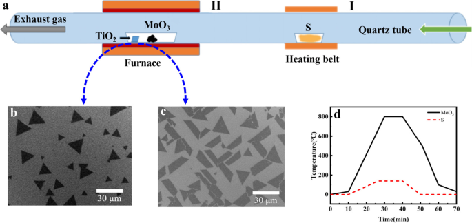
a A set of the CVD system with two temperature zones, I and II. b, c SEM images of ML MoS2 patterns on rutile-TiO2(001) substrate with triangular and belt-like shapes, respectively. d The temperature curve of MoO3 and S are set during the growth of the belt-like ML MoS2
Firstly, the crystal structure of the as-grown MoS2 with triangular and belt-like shapes is characterized by transmission electron microscopy (TEM) and scanning transmission electron microscopy (STEM), respectively. Figure 2a and b show bright-field TEM images of the belt-like and the triangular MoS2 transferred onto the carbon-coated copper grids, respectively, where a quasi-rectangular and triangular geometry can be distinguished, as labeled by the red contour lines. The left and right panels in Fig. 2c show the corresponding selected area electron diffraction (SAED) patterns taken at any location (except for the edge of the ML MoS2) of the belt-like and triangular MoS2, both displaying only one set of hexagonal spots as labeled by red lines in Fig. 2c and suggesting the single crystal nature of the two geometrical MoS2. This indicates that there are no defects in the entire belt-like and triangular MoS2 samples. A typical high-resolution TEM (HRTEM) image of the basal plane (labeled by a rectangle in Fig. 2a) of the belt-like MoS2 is shown in Fig. 2d, which exhibits a hexagonal lattice arrangement with interplanar spacing of 2.7 and 1.6 Å (see a superimposed atomic structure model), corresponding to the (100) and (110) planes, respectively. This further confirms the single crystal nature of the ML MoS2 flakes on the TiO2(001) surface.
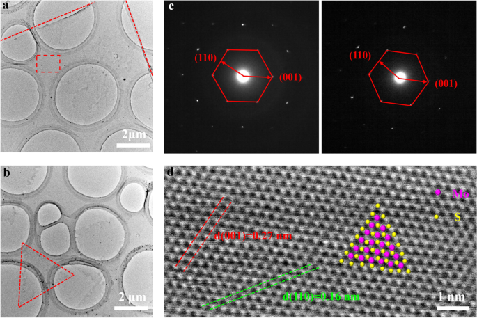
a, b Bright-field TEM images of the MoS2 flakes with the belt-like and triangle shape after transferred on a carbon-coated copper grid. The geometrical contour is labeled by the red rectangle and triangle, respectively. c The left and right panels are the SAED patterns from a and b, respectively. d The HRTEM image of the center region (the dashed line rectangle of a) of the MoS2 belt structure from a, wherein an atomic model of ML MoS2 structure is superimposed
The analysis of the elemental composition
The elemental composition of these belt-like and triangular ML MoS2 patterns was further confirmed with XPS. Figure 3a and b show the deconvoluted XPS spectra, revealing the chemical bonding states of Mo and S of the as-grown ML belt-like MoS2 patterns on TiO2 and of those samples transferred onto SiO2 surface, respectively. For the case of as-prepared ML MoS2 patterns on TiO2 in Fig. 3a, two dominant peaks at 230.83 eV and 233.92 eV appear in the core-level spectrum of Mo 3d of Mo4+, attributed respectively to the doublets Mo 3d5/2 and Mo 3d3/2, which is consistent with the literatures which report on the ML MoS2 [39, 40]. Similarly, two peaks positioned at 230.02 eV and 233.18 eV in the XPS spectrum (Fig. 3b) from transferred ML MoS2 structures onto SiO2/Si surface similarly originate from Mo 3d5/2 and Mo 3d3/2, respectively. At the binding energy (BE) of 228.02 eV (Fig. 3a) and 227.23 eV (Fig. 3b), a typical dome-shape peak can also be seen in both XPS spectra, indicating the S component of MoS2 and belonging to S2s [40]. Besides, tiny amounts of Mo5+and Mo6+ from a relative high BE region were identified, which might be owing to the air-induced oxidation of MoS2 at the defect sites. However, it is worth noting that two Mo 3d peaks and one S 2s peak of the as-grown MoS2 patterns on TiO2 substrate exhibit a blue shift of around 0.8 eV compared to those from the samples transferred onto the SiO2 surface. This might be ascribed to the formation of the semiconductor interface of MoS2/TiO2 due to the difference in work functions of the MoS2 and TiO2 surface. To check the existence of the MoS2/TiO2 interface, the core-level spectra of Ti 2p and O 1s were examined on the blank rutile-TiO2 (the black curve) and on the MoS2-covered TiO2 surface (the red curve) as shown Fig. 3c and d. It is clearly shown that two peaks of Ti 2p and the O 1s peak are synchronously blue-shifted to the higher BE by approximately 0.6 eV for the MoS2-covered TiO2 substrate. The BE blue shift in different elements of the XPS spectra evidence the interface of MoS2/TiO2, which may result in the charge transfer between MoS2 and the substrate and affect thus the PL properties of MoS2 on TiO2 [41,42,43].
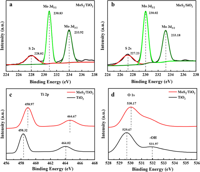
a, b Normalized Mo 3d spectra of as-prepared MoS2 monolayer belt-like structures on Rutile-TiO2(001) substrate and of transferred MoS2 onto SiO2/Si surface, respectively. c, d XPS spectra of Ti2p (c) and O1s (d) collected on as-prepared MoS2/TiO2 (red curve) and on the Rutile-TiO2 (black curve)
The measurements of Raman and PL spectroscopy
After that, we investigate the effect of the interface of MoS2/TiO2 heterostructures on the Raman vibration of the belt-like ML MoS2 on TiO2 substrate by comparing the Raman spectroscopy measurement of the belt-like and triangular ML MoS2 on TiO2(001) and those samples transferred onto SiO2/Si surface. Interestingly, the Raman spectrum from the belt-like patterns and the triangular ones are remarkably different, as shown by the red curve and the black one in Fig. 4a. Two prominent peaks in the red Raman spectrum from the belt-like MoS2 were observed at 385.16 cm−1and 404.14 cm−1, corresponding to the in-plane mode of \({E}_{2g}^1\) and out-of-plane mode of A1g from the single layer MoS2, respectively. The single layer thickness of the belt-like MoS2 structure was confirmed by the atomic force microscopy (AFM) image, as shown in the Supporting Materials as Fig. S1. We can see the distance between the belt-like MoS2 structure and the TiO2 substrate is about 0.71 nm from the profile in Fig. S1b, very close to the thickness of single layer MoS2. Compared to the \({E}_{2g}^1\) mode at 383.16 cm−1 and A1g mode at 404.14 cm−1 detected from the triangular MoS2 structure shown by the black curve, the \({E}_{2g}^1\) mode from the ML MoS2 belt shifts to high energy by about 2 cm−1. However, the Raman spectra of the MoS2 belt and triangular patterns transferred onto SiO2/Si simultaneously exhibit two peaks at 383.66 and 404.14 in Fig. 4b. Meanwhile, it is found that the Raman vibration modes for the transferred ML MoS2 structures are independent of each individual shape. More importantly, the Raman spectrum of the triangular ML MoS2 on TiO2 (the black curve on Fig. 4a) is very analogous to those of the transferred samples on SiO2/Si. This implies that the \({E}_{2g}^1\) peak from the belt structure is blue-shifted compared to that of samples transferred on SiO2/Si surface. Owing to the former studies, the energy shift in the \({E}_{2g}^1\) peak can be generated by the lattice distortion under the in-plane strain [33, 44,45,46,47]. Moreover, it is reported that the peak of the \({E}_{2g}^1\)mode commences a red-shift and even splits into two sub-peaks with increasing the in-plain tensile strain [33, 44,45,46,47]. In our case, the \({E}_{2g}^1\) peak from the belt structure is blue-shifted compared to that of the triangular structure, opposite with most changes (red-shifts) under the tensile strain [26, 33], which might be resulted from an in-plane compressive strain during the growth of the monolayer belt structure confined by the TiO2 crystalline orientation as reported other substrates [48, 49]. The detailed growth mechanism of the substrate-confined belt-like ML MoS2 will be discussed elsewhere [50]. Meanwhile, based on the previous conclusion on the shift value of the Raman vibration mode with strain [26, 33, 37], we can deduce the compressive strain is about 0.3–0.6% in the ML MoS2 belt structure in our case. In view of the similar Raman vibration modes for triangular ML MoS2 on TiO2 and on SiO2/Si surface, it seems that the triangular ML MoS2 on TiO2 surface is in free-strain status. It is easily understandable that the strain can be released for the growth of the triangular ML MoS2 patterns, which are indpendent on the substrate. Accordingly, the Raman vibration modes of the transferred MoS2 structures with the belt-like and triangular shapes do not depend on their individual geometry.
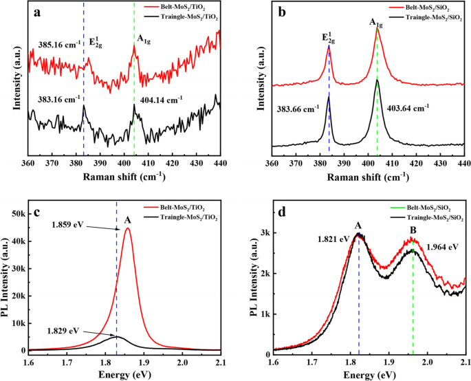
a, b Raman spectra of ML MoS2 belts (the red curve) and triangular ML MoS2 structures (the black curve) on TiO2 substrate and of those samples transferred onto a SiO2/Si substrate, respectively. c, d Photoluminescence (PL) spectra of as-prepared ML MoS2 with the belt-like (the red curve) and triangular (the black curve) shape on TiO2 substrate and on SiO2/Si surface, respectively
Finally, we deeply explore the optical properties of the ML MoS2 belt-like structure tuned by the strain and the interface of MoS2/TiO2 heterostructure via PL spectroscopy. Fig. 4c shows the PL spectrum detected in the strained ML MoS2 belt and free-strain triangular structures on TiO2(001) surface. It is obvious that the PL spectrum of the MoS2 belt (the red curve) is completely different from that of the triangular structure presented by the black curve. The principal PL peak (A peak) in the strained ML MoS2 belt at approximately 1.859 eV (the red curve in Fig. 4c) is due to a direct transition at the K point [1, 2]. The B peak originated from a direct transition between the conduction band and a lower lying valence band, which is obscured in our case owing to a strong PL intensity in A peak. However, the A peak of the black curve in the triangular ML MoS2 structures, being located at 1.821 eV, is relatively weak with an intensity decreased by about ten times than that of the peak A in the strained belt structure. Moreover, the peak A in the red PL spectrum is in a blue shift at about 30 meV compared to that in the black PL spectrum. To visualize the spatial photoluminescent feature, PL mapping in the whole belt structure was executed respectively at the energy of 1.859 eV and 1.821 eV for the as-grown and the corresponding sample transferred on SiO2/Si surface, as shown in Fig. S2a and 2b. The PL mapping images display a belt shape with a uniform photoemission intensity in the whole structure. Moreover, the integral intensity of the belt-like MoS2 on TiO2(001) surface is much higher of ten times than that of belt-structure on SiO2/Si surface, evidenced by the color bars in Fig. S2a and 2b.
According to the previous studies on the strain engineering the band gap transition of monolayer and bilayer MoS2 [33, 51,52,53], the blue shift of the A peak is still induced by the in-plain compressive strain, which is in consistence with our Raman results. Based on the relationship of the energy shift value of the peak A with the strain reported before [26, 33, 37, 53], the strain introduced to the ML MoS2 belt on the TiO2 substrate is in the range of 0.3–0.6%, similar to what have been obtained from the blue-shift in Raman \({E}_{2g}^1\) mode. PL spectra in Fig. 4d obtained in the transferred ML MoS2 structures with different shapes on SiO2/Si further show that common PL traits observed in the red curve and the black one with the same intensity peak A and B, projecting at about 1.821 eV and 1.964 eV, respectively. Moreover, the intensity of peak A is severely dropped down by almost 15 times than that of the strained belt structure on TiO2(001). In other words, the intensity of the peak A in the strained belt-like ML MoS2 on TiO2(001) surface is upgraded by 15 times compared to that of the ML MoS2 belt on SiO2/Si surface. The enhanced PL intensity and the blue-shift of the PL peak A in the as-grown ML belt structure can be ascribed to the strain effect and the charge transfer between the MoS2/TiO2 interface, which will be deeply clarified in the following.
Discussions on the PL behaviors in different ML MoS2 patterns on TiO2(001) and SiO2/Si surfaces
It is well-known that the PL properties of TMD materials are intrinsic to their electronic structures and excitonic effects [54, 55]. To fully understand the increased PL intensity and the blue-shift in PL peak A position for the strained MoS2 belts, the PL spectra from the ML MoS2 belt and the triangular ML MoS2 structures, respectively shown in Fig. 5a and b, are deconvoluted into the neutral exciton peak (A0, the blue peak) and the negative trion peak (A−, the green peak) based on the Gaussian function fitting. Sequentially, we can quantitatively extract the peak position and PL intensity of A0 exciton and A− trion based on the fitting lines. More intuitively, the relationship of the peak A position of the as-grown ML MoS2 on TiO2 and those samples transferred on the SiO2/Si surface with the strain is summarized in Fig. 5c. With increasing the strain, the blue shift (~ 30 meV) emerges in the peak A position of the as-grown belt structure, suggesting an enlarged optical band gap. This phenomenon can be understood that the compressive stain may induce an up-shift in the conduction band minima (CBM) at the K-point and a down-shift in the local valence band maxima (VBM) at the Γ-point. Accordingly, the optical band gap ban be broadened, which has been predicted in the former theoretical results [33, 37, 51, 56, 57]. Under the influence of the strain, the PL intensity for the belt-like and triangular samples on the TiO2 surface exhibits an overt dissimilarity. To understand the intensity disparity, we should consider the many-body complexes in 2D TMD materials tuned by the strain and different interfaces [54, 55]. The intensity ratio of (R) of the A− and A0 peak of the as-grown ML MoS2 and the transferred samples with strain is listed in Fig. 5d. Here, R is defined by the function:
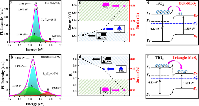
a, b PL spectra of the belt-like and triangular ML MoS2 patterns on TiO2(001) surface were fitted by Gaussian function. The relationship of the energy position (c) and the intensity ratio of A− and A0 (d) of the as-grown and the after-transfer samples with the strain. e, f The structural schematic model of the energy band realignment in the interface between the belt-like MoS2/TiO2 and the triangular MoS2/TiO2, respectively
Among of which \({I}_{A^{-}, AG}\), \({I}_{A^0, AG}\), means the PL intensities of the A− trion and A0 exciton from the as-grown ML MoS2 structures on TiO2, and \({I}_{A^{-},{T}_s}\), and \({I}_{A^0,{T}_s}\) means the A− trion and A0 exciton from the transferred triangular structures on SiO2/Si surface, respectively. This A− and A0 intensity ratio from as-grown structures on TiO2 is normalized by the A− and A0 intensity ratio in the free-strain ML triangular MoS2 structure to compare the strain effect on the A− trion density in different samples. The deconvoluted PL spectra of the transferred samples onto SiO2/Si surface are provided in Fig. S3. According to the above definition of R, the A− and A0 intensity ratio (R) from the transferred samples on SiO2/Si is itself, that is to say, the value of R should be 1. From Fig. 5d, we find that R is decreased down to 50% for the as-grown belt structure under a large compressive strain compared to the as-grown triangular structure. This implies that the trion density of the as-grown MoS2 belt is lower than that of the as-grown triangular one and the transferred samples, which absolutely help to upgrade the PL intensity. The reduced trion is generally attributed to the decreased electron carrier concentration, originating from the interface charge transfer. Due to the strained belt-like structure on TiO2(001) surface, the energy band structure in the interface of MoS2/TiO2 will be realigned as shown by the band structural schematic model in Fig. 5e, which is ascertained by the band gaps of TiO2(001) [58] and the optical band gap tested from our PL measurement. According to Fig. 5e, it is found that the Fermi level of the interface is far from the CBM of the MoS2. Under these circumstances, the charge transfer from the n-type TiO2 substrate to the ML MoS2 belt will be effectively suppressed [58], which results in the reduction of the charged exciton (trion). Conversely, the triangular ML MoS2 without a strain, the energy band realignment is different from that of the large-strain ML MoS2 belt, as shown by Fig. 5f. In this case, the Fermi level of the interface is close to the CBM of MoS2 and the electron carrier transfer easily happen from the TiO2 substrate to the MoS2 ML. As a result, the trion concentration in the as-grown triangular structure is larger than that in the belt structure. Consequently, the PL intensity in the as-grown ML MoS2 belt is increased by 5 times for that in the triangular structure and by 15 times for that in the free-strain transferred samples. Our results are the first time to report that the PL intensity can be extremely upgraded by the compressive strain, opposite with the former results on PL intensity reduction with an increased tensile strain.
Conclusion
In summary, monolayer (ML) MoS2 belt-like single crystals were directly fabricated on Rutile-TiO2(001) surface via CVD, and their PL properties strongly tuned by the strain, the interface of MoS2 and TiO2 and the charge transfer between them. We observe an increased optical band gap and a stronger PL intensity of the as-grown ML MoS2 nanostructures than those transferred on SiO2/Si substrate. The optical band gap is broadened by about 30 meV and the PL emission intensity is enhanced by nearly 15 times for the as-grown ML MoS2 belt-like crystals on TiO2 compared to those on SiO2/Si substrate. This has been explicated by the strain that induces the up-shift in CBM and down-shift in VBM in K-space as well as the energy band structural realignment in the interface of MoS2/TiO2. From this, the charge transfer from TiO2 to MoS2 is effectively inhibited in the strained ML MoS2 belts and the concentration of charged excitons (trion, A−) is thus suppressed, which finally benefit the enhancement of the PL emission intensity. The substrate-confined ML MoS2 belts provide a new way for tailoring many-body complexes and light−matter interactions to upgrade their weak quantum yields and low light absorption, which would be useful for the realization in optoelectronic and nanophotonic devices.