The advancement of molecular-based electronic devices over the past two decades has been spectacular. Despite extensive experimental and theoretical effort, many aspects of fundamental understanding and practical challenges have remained unresolved and prevented the realization of molecular devices. The molecular backbone, the electrode, and the interface between molecular device and electrode are all key factors for the design of molecular devices with unambiguous functionality. Quantum interference and imperfect engineering can be technologically important to modulate the conducting behavior of the molecular junctions. Contrast trends in conducting properties are often obtained intentionally or unintentionally due to anomalous charge transport mechanisms at molecular scale. We briefly summarize four types of counterintuitive transport phenomena which provide vibrant guiding principle for the design of molecular junctions. The future of molecular electronics is definitively bright.
1 Unconventional tunneling length-dependent trends in electron transport
1.1 Collapse of the tunneling behavior on silicon surface
When the tip of scanning tunneling microscope (STM) approaches the silicon surface in the near-to-contact region, substantial decreases of the conductance are observed on both silicon (111) 7 × 7surface [1] and silicon (100) 2 × 1 surface [2] (Fig. 1). Both σ state from silicon adatom in the former case and π state from silicon dimers in latter one (Fig. 1) show strong charge redistributions and their contributions to conductance are considerably reduced. Such unusual feature of conductance drop can be reduced or eliminated by hydrogen terminations. On the other hand, the suppressed transport phenomena may be explored for insulating components which is of paramount importance for optimization of transistors, due to the inherent energy inefficiencies caused by leakage currents in molecular scale devices.

Conductance drop on silicon (100) 2 × 1 surface is obvious on clean model with buckled dimers (S2) but disappeared on hydrogen-terminated model (S1). Reprinted with permission from ref [2]. Copyright 2011 American Chemical Society
1.2 Dominant interference effect in cross-conjugated molecules
Counterintuitive trend in length-dependent electron transfer has been demonstrated in cross-conjugated and linearly conjugated molecules [3, 4]. Long molecules (linearly conjugated) conduct better than short molecules (cross-conjugated) do. This is due to the destructive quantum interference (DQI) dominant in cross-conjugated molecules and large transmission dip present around the Fermi level, reminiscent of meta-connected benzene ring.
1.3 Anti-ohmic behavior with negative decay factor
A positive decay factor β is adopted to describe the tunneling transport behavior of molecular wires. However, the reversed length trend (anti-ohmic) with negative decay factor has been widely explored in both experimental and theoretical work recently [5,6,7,8,9,10,11,12,13,14,15,16,17,18,19,20,21,22,23,24,25,26,27,28,29]. The representative results are summarized in Figs. 2 and 3. For linear carbon chain, inverted bond alternation is key to achieving anti-ohmic behavior [8, 24]. For conjugated compounds with high diradical character [15], the wire conductance increases with length. The external conditions, such as bias (M7 [9] and M30 [25]) and solvent polarity (M29 [24]), have been employed to tune the absolute value of β, shown in Fig. 3. Generally, the evolution of highest occupied molecular orbital (HOMO)-lowest unoccupied molecular orbital (LUMO) gap and Fermi level pinning with molecular length is taken to understand the anti-ohmic character. It should be mentioned that single-particle electronic structure calculations (density functional theory, DFT) failed to capture/predict the anti-ohmic behavior which occurs in excited states only [17].

Atomic models for molecular wires with anti-ohmic behavior. The subscripts “theo” or “exp” define the models from theoretical or experimental work
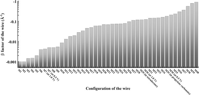
The negative decay factor β for atomic models in Fig. 2
2 Beyond Kirchhoff’s superposition law
Conductance of parallel molecules may not be the conductance sum of the individual molecule (invalid of Kirchhoff’s superposition law), as the collective/cooperative effects (constructive quantum interference (CQI) or destructive quantum interference (DQI)) can arise from adjacent molecules [30]. The CQI of parallel molecules beyond Kirchhoff’s law is first verified experimentally by metal-molecular-metal junctions by choosing benzene as the double-backbone or single-backbone [31]. It has been analytically demonstrated that CQI will lead to a maximum fourfold increase in conductance of parallel molecular junctions [30]. This value could be promoted to 50-fold by coexisting interchannel gating effect and CQI in a tetracationic cyclophane with parallel channels compared with a single channel [32]. By changing connectivity to molecular cores and π stacking modes, 25-fold conductance enhancement could be achieved in an anthanthrene dimer in comparison with a monomer [33]. Furthermore, through-bond and through-space with different quantum interference (QI) patterns have been combined to construct multivalued quantum-interfered states in ortho-pentaphenylene-based junctions [34].
In all carbon molecular junctions, the deviation of Kirchhoff’s superposition law is also demonstrated when the distance between the two carbon atomic wires is smaller than 15.5 Å [35]. By investigating the conductance of the seamless carbon junctions consisting of single and double polyacene molecules bridging carbon nanotubes or graphene nanoribbons, the conductance superposition rule is dependent on the molecular conduction channels, the carbon electrodes, and the interfaces between the molecule and electrode [22] (Fig. 4). Fine Kirchhoff’s law is only found in the junctions where the edge states of the electrode dominating the transport behavior [22] (Fig. 4).

Nonadditive and additive transport in all carbon double-channel single-molecule circuits. The models in the upper panel are double polyacene (PA) bridging carbon nanotube (CNT) electrodes which deviate from Kirchhoff’s circuit laws. The lower models are double PA bridging zigzag graphene nanoribbon (GNR) electrodes which fulfill the linear conductance superposition rule. Reprinted with permission from ref [22]. Copyright 2016 American Chemical Society
3 Dual roles of imperfect engineering in graphene-based molecular junctions
Following the imperfect engineering in conventional silicon electronics, impurity doping (including a single N/B-atom substitution and pyridine-like N-atom substitution) has also been introduced to graphene-based molecular junctions [18]. The texture of imperfect is indeed tricky and it exhibits dual roles, from improving to suppressing carrier transport, according to the variation of imperfect position and molecular length (Fig. 5). For example, single N-atom substitution displayed two opposite roles in affecting electron transport properties: suppressing/enhancing the molecular conductance when the length of polyacene (PA) longer/shorter than a certain value. For dopant at U/D positions, the critical length is equivalent to that of PA with four/five aromatic rings (PA4/PA5) [18]. The imperfection changes the molecular state alignment and coupling to the electrode states and, intuitively, tips the equivalence between two eigenchannels at the Fermi level as shown in Fig. 5. For example, the transmission coefficients of the two channels (T1 and T2) for pristine PA3 are nearly equal, 0.444 and 0.406, respectively. Once single N-atom doped at D1 position of PA3, T1 and T2 are changed to 0.971 and 0.151, respectively. The doped conductance value is enhanced compared to the pristine case. Whereas for pristine PA8, T1 and T2 are 0.997 and 0.968, respectively. When single N-atom substituted at D4 position of PA8, T1 and T2 are changed to 0.997 and 0.418, respectively. The doped conductance value is reduced compared to the pristine counterpart. As a result, imperfect engineering exhibits dual roles in affecting molecular conductance. This rule is an essential reference for designing optimum graphene integrated circuit at the molecular scale. Unambiguous role of imperfect could be achieved with elaborately doping control, which is within the current experimental scope: pattering and doping on graphene with precise atomic level control (chemical vapor deposition [36] and ion irradiation [37, 38]).

Illustration of defect engineering introduced to graphene-based ultrasmall molecular junctions. “U” and “D” denote the positions of H defect or doping. The widths of arrows in each junction qualitatively represent the values of transmission coefficients for the two eigenchannels at Fermi level contributing to the conductance. Reprinted with permission from ref [18]. Copyright 2016 Tsinghua University Press and Springer-Verlag Berlin Heidelberg
4 Masked quantum interference
Quantum interference (QI) is of particular important to molecular electronics and provides unique opportunities for tuning the conductance through manipulation of the electron wavefunction. For example, the developed reversible switching between CQI and DQI by protonation and deprotonation (chemical gating) of the pyridine core [39] could modulate the conductance by one order. Another representative example is the metal-phenyl ring-metal junctions, where para-coupled samples illustrate CQI (high conductance) and meta-coupled cases exhibit DQI (low conductance) [40]. However, the through-space interactions could reverse such contrast behaviors, namely, meta-connected benzene with CQI and para-connected one with DQI [41]. The “imperfect” interference by masking of through-space interactions should be taken into account in designing metal-π-system molecules-metal junctions.
Slotted carbon nanotube with parallel paths may be alternate performing systems to manipulate the QI phenomena (Fig. 6). Both normal electric [42] and flexoelectric fields [43] could break the degeneracy of frontier orbitals of the parallel paths and tune the crosstalk between them. Thus, the external stimuli could open and linearly tune Fano resonance in such junctions with parallel arrangement.

Normal electric and flexoelectric fields tunable Fano resonance based on CNT junctions with parallel paths. Reprinted with permission from ref [43]. Copyright 2021 American Association for the Advancement of Science
5 Conclusion and perspectives
We have summarized recent progress in the field of molecular electronics, with a specific focus on the “counterintuitive” results in the charge transport across molecular junctions. The anti-ohmic wires are highly desirable as interconnects in molecular circuitry [6]. A definite role of imperfect could be achieved with precise atomic doping [38]. To avoid the masking effect of through-space interactions, the carbon junctions with parallel paths are prominent to serve as a stable platform for tunable quantum interference by both normal electric and flexoelectric fields [43].